


-
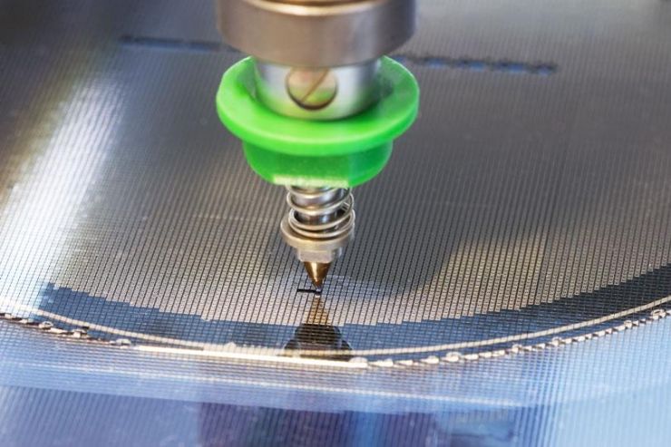
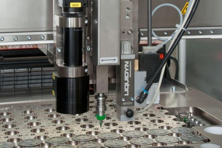
Die Bonding
Infotech’s solutions for die bonding are not limited to the classical separation and packaging of semiconductor chips. More and more additional process steps are combined with die bonding. Our die bonding modules from the Component Matrix lend themselves well to be combined with dispensing, handling, joining, assembling and many other applications, in place of using multiple, specifically task-dedicated machines.
We handle wafer sizes from 4“up to 12“on different frame formats. The large flexibility, which our platforms offer, is supported by the in-house developed application software VisualMachinesTM. The functions refer to the SEMI-standards but can also be adapted to the customer needs.
Our die bonding solutions are predestined for the assembly of LED products, sensors, MEMS, VCSEL diodes and power semiconductors. Die sizes down to 200 µm from wafer, chip-on-chip and chip-on-wafer applications belong to our range of service.
Further information die bonding machines:
Products - Die Bonding -
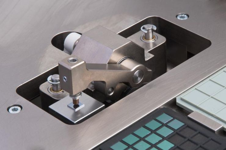
Flip-Chip Bonding
In flip chip bonding processes, chips packaged in BGA (Ball Grid Array) or µBGA respectively are directly connected to the substrate. This procedure is particularly suitable for semiconductor devices with a high number of joints that have the shape of small solder balls (bumps) and are arranged on the bottom side of the housing. The BGA/µBGA is fed upside down to the machine and must be flipped.
Conditions for a successful flip chip bonding are a flipper unit (shown in the photo), high precision alignment of the solder balls to the bond pads as well as the possibility to apply flux by dispensing or dipping. For small batches, prototype assemblies or rework tasks, the use of our well-established hot gas soldering system is recommended.
With machines from Infotech, flip chip bonding can be executed reliably, professionally and if necessary, combined with other high quality process steps.
-
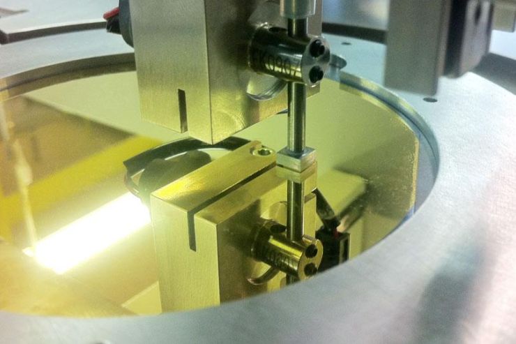
Ultrasonic Bonding
Ultrasonic bonding or thermosonic bonding is another joining technology for the attachment of bumped components or flip chip parts directly on the substrate. Whereby the substrate is fixed and preheated. During the placement of the flip chip, the part is vibrated by the nozzle, which is stimulated by ultrasonic, and pressed with a controlled force onto the substrate. Through the heat which is generated locally by friction of the bumps on the pads, solid fusion joints arise.
Conditions for this joining process are a solid building of the machine and the interaction of process parameters which must be controlled and synchronized. These parameters include substrate temperature, ultrasonic power, bonding force per joint and process time.
With Infotech machines, ultrasonic bonding can be executed reliably, professionally and if necessary, combined with other high quality process steps.
-
Eutectic Bonding
The principle of eutectic bonding has experienced a remarkable rebirth since the upswing of fiber-optic networks. This joining technique, which has been known for a long time, is based on Eutectic alloys (Au-Sn, Si-Au or Ge-Al), which are evaporated on the chip and carrier before bonding. During the bonding process, the metal layers melt under precisely controlled force and temperature without the help of flux and results in the chip being permanently connected to the substrate.
The application is often taken into consideration at the precise assembly of surface emitter (VCSEL diodes) on their submounts. Thereby, the bonder has not only to be able to control the accurate position but also to keep a defined overhang of the emitting edge which is just a few of microns. In addition, the plane-parallelism between diode and carrier also needs to be controlled.
Eutectic bonding is also used for MEMS packaging, chip on-wafer technology and for other wafer based parts.
-
Watch Parts Assembly
Sample Video - Watch Party Assembly
The automated assembly of moving parts, dials and other parts of wristwatches is based on classical semi-automated machines or specialty machines.
As the first company worldwide, Infotech provides the capability for fully automated assembly of a mechanical movement, in collaboration with a famous Swiss watch manufacturer.
Our recipe for success is called the «Infotech Component Matrix», which contains standardized axes, machine components, loading/unloading systems and many more. In the process of assembling complex watch parts such as gear wheels, anchors and balances, we rely on the use of our integrated vision system.
Other less complex watch assembly processes such as the assembly of dials, the gluing of dials and the mounting of watch glasses and many other applications are also included in our range of products and services.


-
Die Bonding
Infotech’s solutions for die bonding are not limited to the classical separation and packaging of semiconductor chips. More and more additional process steps are combined with die bonding. Our die bonding modules from the Component Matrix lend themselves well to be combined with dispensing, handling, joining, assembling and many other applications, in place of using multiple, specifically task-dedicated machines.
We handle wafer sizes from 4“up to 12“on different frame formats. The large flexibility, which our platforms offer, is supported by the in-house developed application software VisualMachinesTM. The functions refer to the SEMI-standards but can also be adapted to the customer needs.
Our die bonding solutions are predestined for the assembly of LED products, sensors, MEMS, VCSEL diodes and power semiconductors. Die sizes down to 200 µm from wafer, chip-on-chip and chip-on-wafer applications belong to our range of service.
Further information die bonding machines:
Products - Die Bonding -
Flip-Chip Bonding
In flip chip bonding processes, chips packaged in BGA (Ball Grid Array) or µBGA respectively are directly connected to the substrate. This procedure is particularly suitable for semiconductor devices with a high number of joints that have the shape of small solder balls (bumps) and are arranged on the bottom side of the housing. The BGA/µBGA is fed upside down to the machine and must be flipped.Conditions for a successful flip chip bonding are a flipper unit (shown in the photo), high precision alignment of the solder balls to the bond pads as well as the possibility to apply flux by dispensing or dipping. For small batches, prototype assemblies or rework tasks, the use of our well-established hot gas soldering system is recommended.
With machines from Infotech, flip chip bonding can be executed reliably, professionally and if necessary, combined with other high quality process steps.
-
Ultrasonic Bonding
Ultrasonic bonding or thermosonic bonding is another joining technology for the attachment of bumped components or flip chip parts directly on the substrate. Whereby the substrate is fixed and preheated. During the placement of the flip chip, the part is vibrated by the nozzle, which is stimulated by ultrasonic, and pressed with a controlled force onto the substrate. Through the heat which is generated locally by friction of the bumps on the pads, solid fusion joints arise.
Conditions for this joining process are a solid building of the machine and the interaction of process parameters which must be controlled and synchronized. These parameters include substrate temperature, ultrasonic power, bonding force per joint and process time.
With Infotech machines, ultrasonic bonding can be executed reliably, professionally and if necessary, combined with other high quality process steps.
-
Eutectic Bonding
The principle of eutectic bonding has experienced a remarkable rebirth since the upswing of fiber-optic networks. This joining technique, which has been known for a long time, is based on Eutectic alloys (Au-Sn, Si-Au or Ge-Al), which are evaporated on the chip and carrier before bonding. During the bonding process, the metal layers melt under precisely controlled force and temperature without the help of flux and results in the chip being permanently connected to the substrate.
The application is often taken into consideration at the precise assembly of surface emitter (VCSEL diodes) on their submounts. Thereby, the bonder has not only to be able to control the accurate position but also to keep a defined overhang of the emitting edge which is just a few of microns. In addition, the plane-parallelism between diode and carrier also needs to be controlled.
Eutectic bonding is also used for MEMS packaging, chip on-wafer technology and for other wafer based parts.
-
Watch Parts Assembly
Sample Video - Watch Party Assembly
The automated assembly of moving parts, dials and other parts of wristwatches is based on classical semi-automated machines or specialty machines.
As the first company worldwide, Infotech provides the capability for fully automated assembly of a mechanical movement, in collaboration with a famous Swiss watch manufacturer.
Our recipe for success is called the «Infotech Component Matrix», which contains standardized axes, machine components, loading/unloading systems and many more. In the process of assembling complex watch parts such as gear wheels, anchors and balances, we rely on the use of our integrated vision system.
Other less complex watch assembly processes such as the assembly of dials, the gluing of dials and the mounting of watch glasses and many other applications are also included in our range of products and services.
e.


